
Wafer Level Packaging Market Report
First published: 24 September 2024 | Last updated: 31 January 2026 | Report Code: wafer-level-packaging
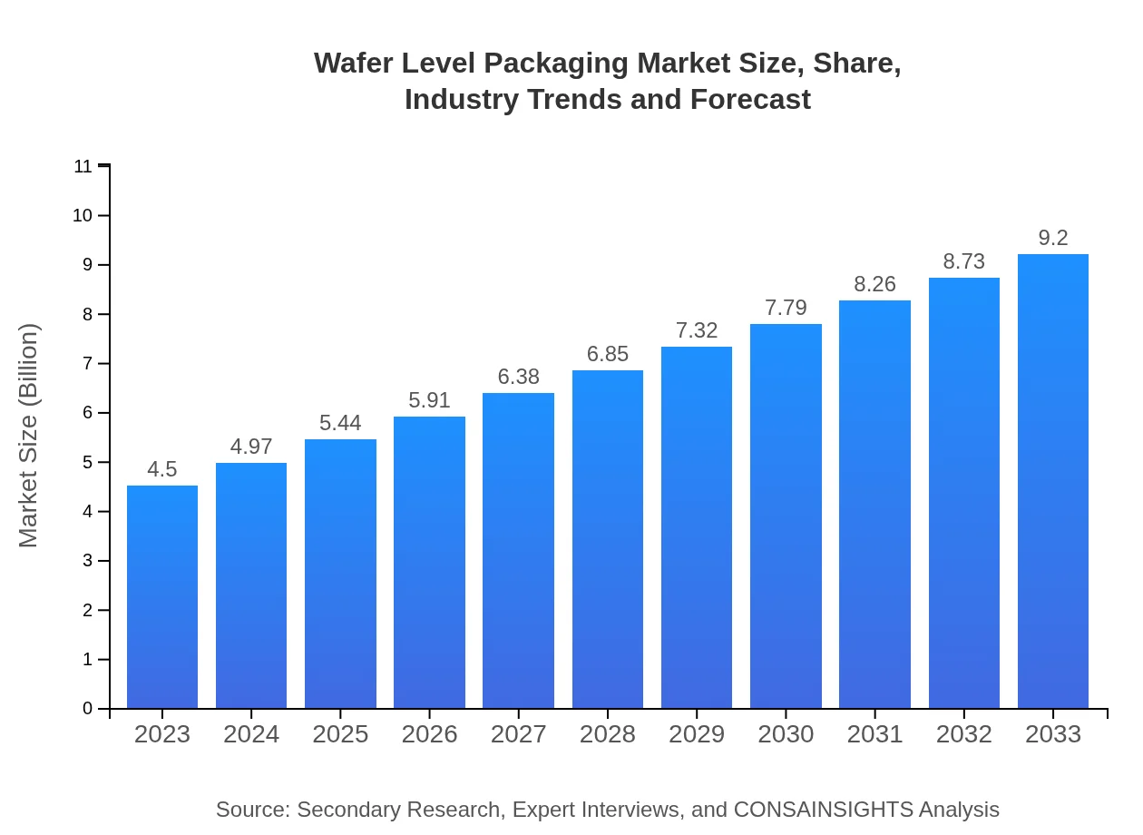
Wafer Level Packaging Market — USD $4.5 Billion in 2023, Growing to USD 9.20null by 2033 at 7.2% CAGR
This report provides an in-depth analysis of the Wafer Level Packaging market from 2023 to 2033, detailing market size, growth forecasts, segmentations, regional dynamics, and industry trends to offer actionable insights for stakeholders.
| Metric | Value |
|---|---|
| Study Period | 2023 - 2033 |
| 2023 Market Size | $4.50 Billion |
| CAGR (2023-2033) | 7.2% |
| 2033 Market Size | $9.20 Billion |
| Top Companies | Samsung Electronics, Intel Corporation, TSMC, Amkor Technology, STMicroelectronics |
| Published Date | 24 September 2024 |
| Last Modified Date | 31 January 2026 |
Wafer Level Packaging Market Overview
Customize Wafer Level Packaging Market Report market research report
- ✔ Get in-depth analysis of Wafer Level Packaging market size, growth, and forecasts.
- ✔ Understand Wafer Level Packaging's regional dynamics and industry-specific trends.
- ✔ Identify potential applications, end-user demand, and growth segments in Wafer Level Packaging
What is the Market Size & CAGR of Wafer Level Packaging market in 2023?
Wafer Level Packaging Industry Analysis
Wafer Level Packaging Market Segmentation and Scope
Tell us your focus area and get a customized research report.
Wafer Level Packaging Market Analysis Report by Region
Europe Wafer Level Packaging Market Report:
Europe's Wafer Level Packaging market, valued at $1.27 billion in 2023, is expected to grow to $2.61 billion by 2033. The region benefits from advanced manufacturing capabilities and a growing emphasis on research and development in packaging technologies, principal in automotive and high-performance computing sectors.Asia Pacific Wafer Level Packaging Market Report:
The Asia Pacific region holds a significant share of the Wafer Level Packaging market, valued at approximately $0.85 billion in 2023, expected to reach $1.73 billion by 2033. This growth is attributed to the presence of major semiconductor manufacturers and a robust consumer electronics market, particularly in countries like China, Japan, and South Korea, which are leading technological advancements and innovation in electronics.North America Wafer Level Packaging Market Report:
North America is projected to exhibit substantial growth in the WLP market, from $1.72 billion in 2023 to $3.52 billion by 2033. This increase is fueled by significant investments in technological innovations and demand for advanced electronic systems in automotive and industrial applications, as well as a strong presence of key industry players.South America Wafer Level Packaging Market Report:
In South America, the Wafer Level Packaging market was valued at $0.37 billion in 2023, predicted to grow to $0.76 billion by 2033. The growth in this region is driven by an increasing adoption of smart technologies and expanding telecommunications infrastructure, although it remains comparatively smaller than other markets.Middle East & Africa Wafer Level Packaging Market Report:
In the Middle East and Africa, the Wafer Level Packaging market is valued at $0.28 billion in 2023 and is projected to reach $0.58 billion by 2033. This growth is largely influenced by technological investments in smart devices and communication solutions, albeit facing challenges due to economic variability in the region.Tell us your focus area and get a customized research report.
Wafer Level Packaging Market Analysis By Technology
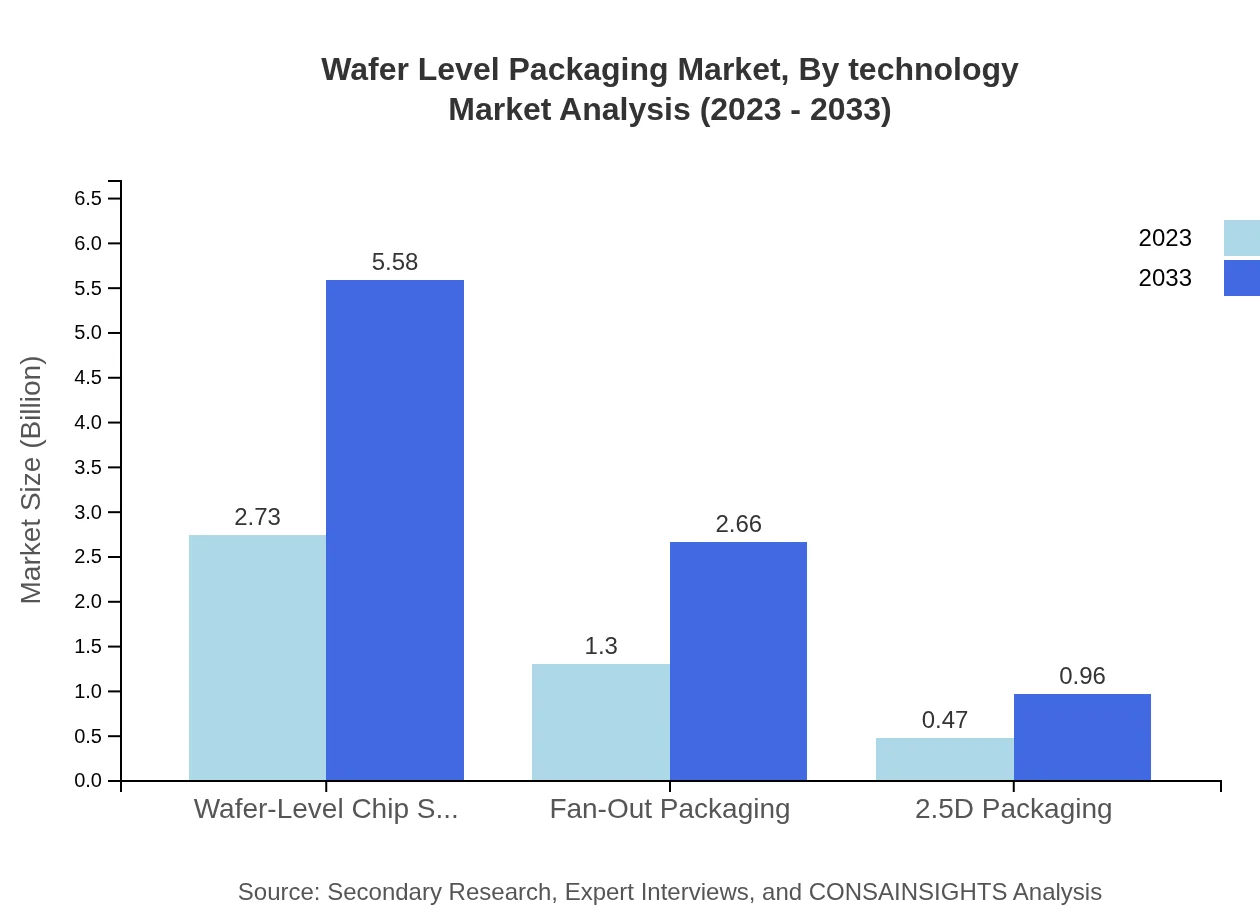
In 2023, Wafer-Level Chip Scale Packaging (WLCSP) leads the market with a size of $2.73 billion, projected to grow to $5.58 billion by 2033, capturing 60.67% market share. Fan-Out Packaging follows with $1.30 billion in 2023, expected to increase to $2.66 billion by 2033, holding a share of 28.91%. Other technologies such as 2.5D Packaging and substrates are also contributing, though they share smaller segments.
Wafer Level Packaging Market Analysis By Application
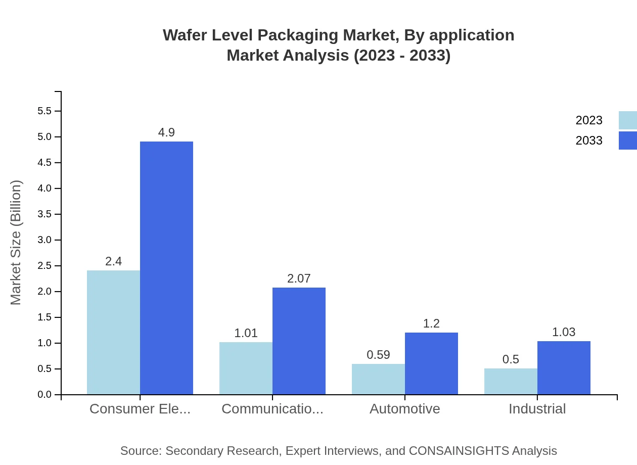
The Consumer Electronics segment dominates the Wafer Level Packaging market, valued at $2.40 billion in 2023 and expected to rise to $4.90 billion by 2033, accounting for 53.3% market share. Communication devices and automotive applications also show promise, with respective sizes of $1.01 billion and $0.59 billion in 2023, growing steadily as industries adopt more compact and efficient packaging solutions.
Wafer Level Packaging Market Analysis By Material

Silicon-based WLP remains predominant due to its established performance and reliability, valued at $2.73 billion in 2023 and slated for growth to $5.58 billion by 2033. Polymer materials, although still emerging, show significant potential, moving from $1.30 billion in 2023 to $2.66 billion by 2033, driven by flexibility and ease of integration into various applications.
Wafer Level Packaging Market Analysis By Product Type
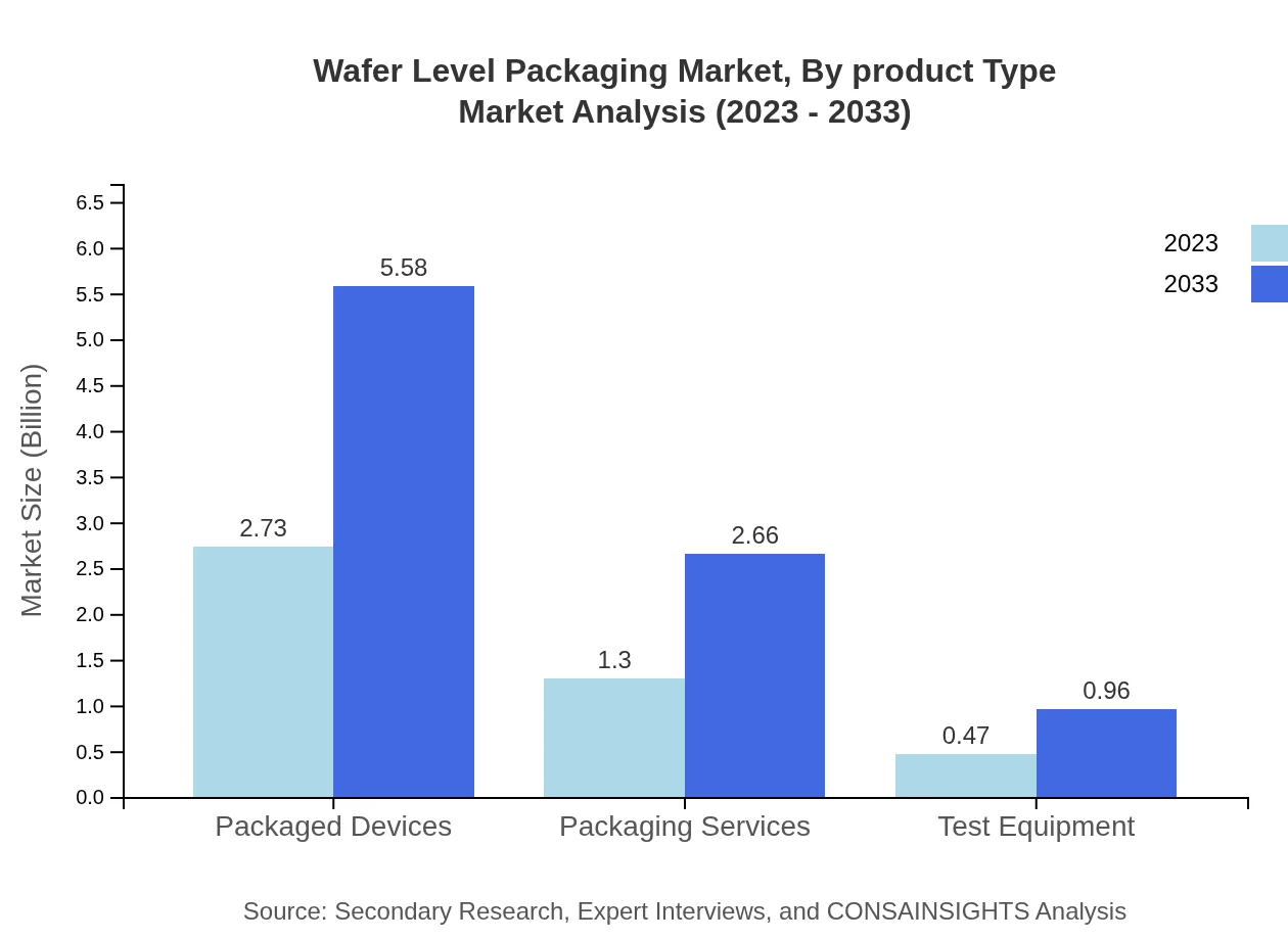
In terms of product types, Packaged Devices lead the segment with $2.73 billion in 2023, expected to grow to $5.58 billion by 2033. Packaging Services and Test Equipment also contribute to the market, reflecting the increasing trend toward integrated solutions and quality assurance in semiconductor manufacturing.
Wafer Level Packaging Market Trends and Future Forecast
Tell us your focus area and get a customized research report.
Global Market Leaders and Top Companies in Wafer Level Packaging Industry
Samsung Electronics:
A leading innovator in the semiconductor industry, Samsung has made significant contributions to WLP technology, focusing on advanced packaging solutions for its powerful electronic devices.Intel Corporation:
Intel invests heavily in packaging solutions to enhance its processor performance, utilizing WLP to minimize size without compromising power efficiency.TSMC:
The world’s largest foundry, TSMC leads in advanced packaging technologies, including WLP, catering to top-tier semiconductor designs globally.Amkor Technology:
Amkor specializes in providing advanced packaging and test services, including WLP, to leading semiconductor companies, enhancing product performance and reliability.STMicroelectronics:
A key player in developing hybrid packaging technologies and applications, STMicroelectronics incorporates WLP in various consumer and industrial products.We're grateful to work with incredible clients.


FAQs
What is the market size of wafer Level Packaging?
The wafer-level packaging market is currently valued at $4.5 billion, with a projected CAGR of 7.2%. By 2033, the market is expected to see substantial growth due to increasing applications in various sectors.
What are the key market players or companies in the wafer Level Packaging industry?
Key players in the wafer-level packaging industry include semiconductor companies and packaging service providers such as Advanced Micro Devices, Intel, and ASE Group. Their innovation drives growth and shapes market dynamics.
What are the primary factors driving the growth in the wafer Level Packaging industry?
Growth is primarily driven by the demand for miniaturization of electronics, advancements in technology, and increasing applications in 5G and IoT products, fostering a shift toward high-density packaging solutions.
Which region is the fastest Growing in the wafer Level Packaging market?
North America is the fastest-growing region, projected to expand from $1.72 billion in 2023 to $3.52 billion in 2033. This growth is fueled by strong demand in consumer electronics and automotive sectors.
Does ConsaInsights provide customized market report data for the wafer Level Packaging industry?
Yes, ConsaInsights offers customized market report data tailored to specific needs within the wafer-level packaging industry, providing insights into market trends, competitors, and opportunities.
What deliverables can I expect from this wafer Level Packaging market research project?
Deliverables include comprehensive reports, market forecasts, competitor analysis, and segmented data insights that help stakeholders make informed strategic decisions in the wafer-level packaging market.
What are the market trends of wafer Level Packaging?
Key trends include the shift towards hybrid packaging solutions, increased integration of Wafer-Level Chip Scale Packaging (WLCSP), and the rise in demand for sustainable materials across various electronic applications.